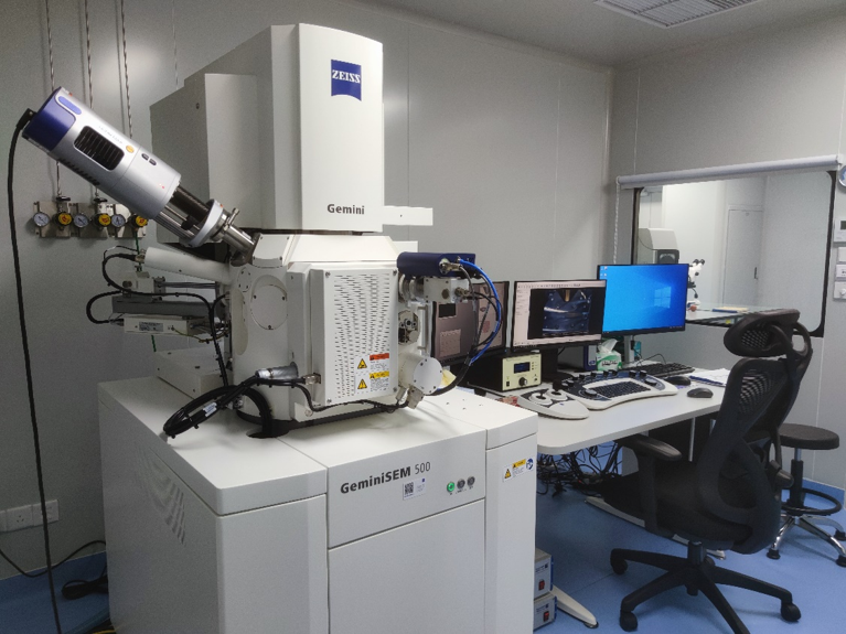
Description: It is used to observe the microstructural and crystal morphologies in a nano-meter scale for polymeric powders, thin films, and bulks. The functions for SEM include elemental analysis, in-situ stress-strain micromechanical experiments.
Model: Gemini500 (Carl Zeiss)
Acceleration voltage: 0.02-30 kV
Working distance: 8.5 mm
Probe current: 5 pA – 20 nA
Resolution: 0.5 nm at 15 kV, 0.9 nm at 1 kV, 1 nm at 500 V
Probe: Equipped with low-/high- secondary electron, backscattered electron probes
Energy spectrometer: UltimMax65 Oxford Energy Spectrometer
Elemental analysis range: Be4 – Cf98
Stretching stage:
Mode: Kammrath & Weiss stage
Load cell: 1 – 500 N
Displacement resolution: 100 nm
Max. length for the clamp: 45 mm
Temperature ragne: -100 – 500 °C
downloadFile